Electron beam-induced deposition
 From Wikipedia the free encyclopedia
Electron-beam-induced deposition (EBID) is a process of decomposing gaseous molecules by an electron beam leading to deposition of non-volatile fragments onto a nearby substrate. The electron beam is usually provided by a scanning electron microscope, which results in high spatial accuracy (potentially below one nanometer) and the possibility to produce free-standing, three-dimensional structures.[1]
Process[edit]
.png)

The focused electron beam of a scanning electron microscope (SEM) or scanning transmission electron microscope (STEM) is commonly used. Another method is ion-beam-induced deposition (IBID), where a focused ion beam is applied instead. Precursor materials are typically liquid or solid and gasified prior to deposition, usually through vaporization or sublimation, and introduced, at accurately controlled rate, into the high-vacuum chamber of the electron microscope. Alternatively, solid precursors can be sublimated by the electron beam itself.[2]
When deposition occurs at a high temperature or involves corrosive gases, a specially designed deposition chamber is used;[3] it is isolated from the microscope, and the beam is introduced into it through a micrometre-sized orifice. The small orifice size maintains differential pressure in the microscope (vacuum) and deposition chamber (no vacuum). Such deposition mode has been used for EBID of diamond.[3][4]
In the presence of the precursor gas, the electron beam is scanned over the substrate, resulting in deposition of material. The scanning is usually computer-controlled. The deposition rate depends on a variety of processing parameters, such as the partial precursor pressure, substrate temperature, electron beam parameters, applied current density, etc. It usually is in the order of 10 nm/s.[5]
Deposition mechanism[edit]
Primary electron energies in SEMs or STEMs are usually between 10 and 300 keV, where reactions induced by electron impact, i.e. precursor dissociation, have a relatively low cross section. The majority of decomposition occurs via low energy electron impact: either by low energy secondary electrons, which cross the substrate-vacuum interface and contribute to the total current density, or inelastically scattered (backscattered) electrons.[5][6][7]
Spatial resolution[edit]
Primary S(T)EM electrons can be focused into spots as small as ~0.045 nm.[8] While the smallest structures deposited so far by EBID are point deposits of ~0.7 nm diameter,[9] deposits usually have a larger lateral size than the beam spot size. The reason are the so-called proximity effects, meaning that secondary, backscattered and forward scattered (if the beam dwells on already deposited material) electrons contribute to the deposition. As these electrons can leave the substrate up to several microns away from the point of impact of the electron beam (depending on its energy), material deposition is not necessarily confined to the irradiated spot. To overcome this problem, compensation algorithms can be applied, which is typical for electron beam lithography.
Materials and precursors[edit]
As of 2008 the range of materials deposited by EBID included Al, Au, amorphous carbon, diamond, Co, Cr, Cu, Fe, GaAs, GaN, Ge, Mo, Nb, Ni, Os, Pd, Pt, Rh, Ru, Re, Si, Si3N4, SiOx, TiOx, W,[5] and was being expanded. The limiting factor is the availability of appropriate precursors, gaseous or having a low sublimation temperature.
The most popular precursors for deposition of elemental solids are metal carbonyls of Me(CO)x structure or metallocenes. They are easily available, however, due to incorporation of carbon atoms from the CO ligands, deposits often exhibit a low metal content.[5][10] Metal-halogen complexes (WF6, etc.) result in cleaner deposition, but are more difficult to handle as they are toxic and corrosive.[5] Compound materials are deposited from specially crafted, exotic gases, e.g. D2GaN3 for GaN.[5]
Advantages[edit]
- Very flexible regarding deposit shape and composition; the electron beam is lithographically controlled and a multitude of potential precursors is available
- Lateral size of the produced structures and accuracy of deposition are unprecedented
- The deposited material can be characterized using the electron microscopy techniques (TEM, EELS, EDS, electron diffraction) during or right after deposition. In situ electrical and optical characterization is also possible.
Disadvantages[edit]
- Serial material deposition and low deposition rates in general limit throughput and thus mass production
- Controlling the elemental or chemical deposit composition is still a major challenge, as the precursor decomposition pathways are mostly unknown
- Proximity effects can lead to unintended structure broadening
Ion-beam-induced deposition[edit]
Ion-beam-induced deposition (IBID) is very similar to EBID with the major difference that focused ion beam, usually 30 keV Ga+, is used instead of the electron beam. In both techniques, it is not the primary beam, but secondary electrons which cause the deposition. IBID has the following disadvantages as compared to EBID:
- Angular spread of secondary electrons is larger in IBID thus resulting in lower spatial resolution.
- Ga+ ions introduce additional contamination and radiation damage to the deposited structure, which is important for electronic applications.[10]
- Deposition occurs in a focused ion beam (FIB) setup, which strongly limits characterization of the deposit during or right after the deposition. Only SEM-like imaging using secondary electrons is possible, and even that imaging is restricted to short observations due to sample damaging by the Ga+ beam. The use of a dual beam instrument, that combines a FIB and an SEM in one, circumvents this limitation.
The advantages of IBID are:
- Much higher deposition rate
- Higher purity
Shapes[edit]
Nanostructures of virtually any 3-dimensional shape can be deposited using computer-controlled scanning of electron beam. Only the starting point has to be attached to the substrate, the rest of the structure can be free standing. The achieved shapes and devices are remarkable:
- World smallest magnet[6]
- Fractal nanotrees[6]
- Nanoloops (potential nanoSQUID device)[6]
- Superconducting nanowires[10]
-
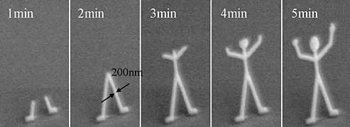 Snapshots of growing a doll-like nanostructure by IBID
 -
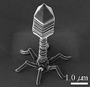 A model of bacteriophage grown by IBID
 -
 A model of Leaning Tower of Pisa grown by IBID
 -
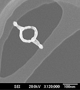 Letter Φ grown by EBID


See also[edit]
References[edit]
- ^ Carden, Will G.; Lu, Hang; Spencer, Julie A.; Fairbrother, D. Howard; McElwee-White, Lisa (2018-06-01). "Mechanism-based design of precursors for focused electron beam-induced deposition". MRS Communications. 8 (2): 343–357. doi:10.1557/mrc.2018.77. ISSN 2159-6867.
- ^ Mura, Francesco; Cognigni, Flavio; Ferroni, Matteo; Morandi, Vittorio; Rossi, Marco (2023-08-24). "Advances in Focused Ion Beam Tomography for Three-Dimensional Characterization in Materials Science". Materials. 16 (17): 5808. Bibcode:2023Mate...16.5808M. doi:10.3390/ma16175808. ISSN 1996-1944. PMC 10488958. PMID 37687502.
- ^ a b Kiyohara, Shuji; Takamatsu, Hideaki; Mori, Katsumi (2002). "Microfabrication of diamond films by localized electron beam chemical vapour deposition". Semiconductor Science and Technology. 17 (10): 1096. Bibcode:2002SeScT..17.1096K. doi:10.1088/0268-1242/17/10/311.
- ^ Nayak, A.; Banerjee, H. D. (1995). "Electron beam activated plasma chemical vapour deposition of polycrystalline diamond films". Physica Status Solidi A. 151 (1): 107–112. Bibcode:1995PSSAR.151..107N. doi:10.1002/pssa.2211510112.
- ^ a b c d e f Randolph, S.; Fowlkes, J.; Rack, P. (2006). "Focused, Nanoscale Electron-Beam-Induced Deposition and Etching". Critical Reviews of Solid State and Materials Sciences. 31 (3): 55. Bibcode:2006CRSSM..31...55R. doi:10.1080/10408430600930438. S2CID 93769658.
- ^ a b c d K. Furuya (2008). "Nanofabrication by advanced electron microscopy using intense and focused beam". Sci. Technol. Adv. Mater. 9 (1): 014110. Bibcode:2008STAdM...9a4110F. doi:10.1088/1468-6996/9/1/014110. PMC 5099805. PMID 27877936.
- ^ M. Song and K. Furuya (2008). "Fabrication and characterization of nanostructures on insulator substrates by electron-beam-induced deposition". Sci. Technol. Adv. Mater. 9 (2): 023002. Bibcode:2008STAdM...9b3002S. doi:10.1088/1468-6996/9/2/023002. PMC 5099707. PMID 27877950.
- ^ Erni, Rolf; Rossell, MD; Kisielowski, C; Dahmen, U (2009). "Atomic-Resolution Imaging with a Sub-50-pm Electron Probe". Physical Review Letters. 102 (9): 096101. Bibcode:2009PhRvL.102i6101E. doi:10.1103/PhysRevLett.102.096101. PMID 19392535.
- ^ Van Dorp, Willem F. (2005). "Approaching the Resolution Limit of Nanometer-Scale Electron Beam-Induced Deposition". Nano Letters. 5 (7): 1303–7. Bibcode:2005NanoL...5.1303V. doi:10.1021/nl050522i. PMID 16178228.
- ^ a b c Luxmoore, I; Ross, I; Cullis, A; Fry, P; Orr, J; Buckle, P; Jefferson, J (2007). "Low temperature electrical characterisation of tungsten nano-wires fabricated by electron and ion beam induced chemical vapour deposition". Thin Solid Films. 515 (17): 6791. Bibcode:2007TSF...515.6791L. doi:10.1016/j.tsf.2007.02.029.
External links[edit]
- "Nanofabrication: Fundamentals and Applications" Ed.: Ampere A. Tseng, World Scientific Publishing Company (March 4, 2008), ISBN 981-270-076-5, ISBN 978-981-270-076-6
- K. Molhave: "Tools for in-situ manipulations and characterization of nanostructures", PhD thesis, Technical University of Denmark, 2004
| Basics | |||||||
|---|---|---|---|---|---|---|---|
| Electron interaction with matter | |||||||
| Instrumentation | |||||||
| Microscopes |
| ||||||
| Techniques |
| ||||||
| Others |
| ||||||